printed circuit board designer
Eco-conscious artist transforms trashed PCBs into stunning sculptures. 9 Images about Eco-conscious artist transforms trashed PCBs into stunning sculptures : Online Advanced PCB Layout Course, by Motherboard Designer - Welldone, Printed Circuit Board Design Services – Asia Pacific Circuits Co. and also Watch routing PCB Layout with DDR3 & High Speed Interfaces - YouTube.
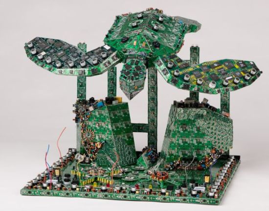
Eco-conscious Artist Transforms Trashed PCBs Into Stunning Sculptures
 www.ecofriend.com
pcbs reciclados discarded conscious trashed karya ecofriend ordenadores atcrux
4 Exciting Innovations In PCB Designs | Future Technology In PCB Design
 www.electronicsandyou.com
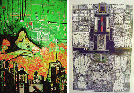
Circuitboard Artwork: A Gallery Inside Your Computer | Urbanist
 weburbanist.com
circuitboard komputer kaskus
Printed Circuit Board Design Services – Asia Pacific Circuits Co.
 www.apc-pcbassembly.com
pads ddr2 gy iic gandhinagar orcad cadence altium infotech sensor quoting infrared
Watch Routing PCB Layout With DDR3 & High Speed Interfaces - YouTube
 www.youtube.com
pcb layout speed circuit routing double guidelines vs lpddr4 ddr3 sided layer integration advantages fpga single using highspeed main interfaces
SOLIDWORKS PCB 2018 Top 5 Enhancements Video
 www.javelin-tech.com
solidworks pcb altium ds innovative enhancements unleashed powered technology sp3 layout schematic interface jyvsoft screenshots crack javelin tech
A Practical Guide To High-Speed Printed-Circuit-Board Layout | Analog
 www.analog.com
noninverting inverting sot
Online Advanced PCB Layout Course, By Motherboard Designer - Welldone
 www.fedevel.com
pcb layout cost orcad motherboard designer software cadence designing circuit printed course advanced cad circuits layer services fedevel capabilities powerful
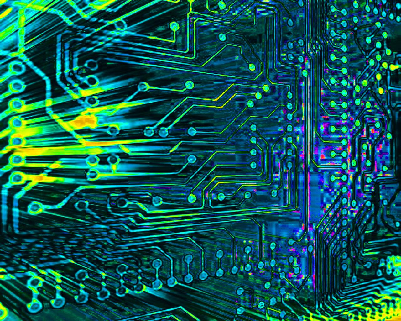
Circuit Board Wallpapers - Wallpaper Cave
 wallpapercave.com
circuit wallpapers desktop computer backgrounds pc printed electronic 1280 pcb background 1024 electronics 1080p definition android wallpapersafari electronique wallpapercave pixel
4 exciting innovations in pcb designs. A practical guide to high-speed printed-circuit-board layout. Solidworks pcb 2018 top 5 enhancements video